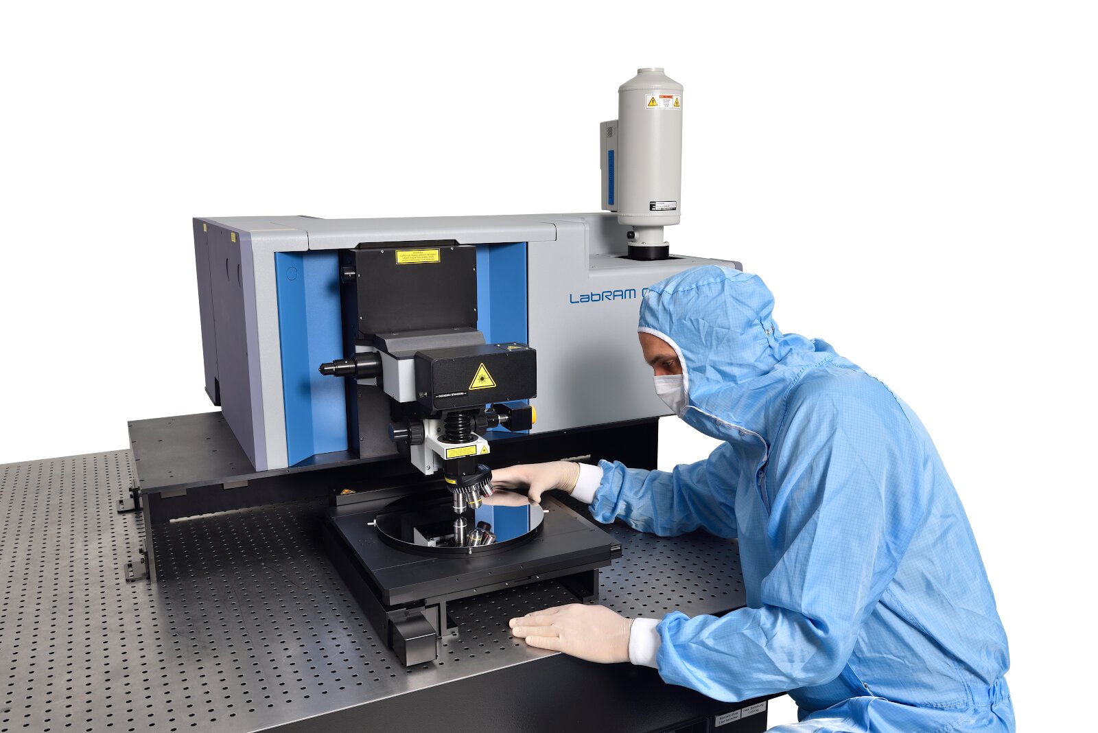
The HORIBA LabRAM Odyssey Semiconductor is a specialized Raman system configured for semiconductor industry metrology, featuring automated wafer mapping, stress/strain analysis, and process control applications.
The HORIBA LabRAM Odyssey Semiconductor is a specialized configuration of the LabRAM Odyssey platform optimized for semiconductor materials characterization and process metrology. It is designed to meet the demands of semiconductor research and manufacturing environments, with features for automated wafer-scale Raman mapping, stress and strain analysis, crystalline quality assessment, and impurity characterization. The system provides sub-micron spatial resolution Raman mapping combined with the spectral precision required to detect small shifts in peak positions that indicate stress, strain, or compositional variation in silicon, germanium, silicon carbide, gallium nitride, and other semiconductor materials. Automated stage routines allow mapping of full wafer or selected die areas with user-defined grid density. The LabRAM Odyssey Semiconductor can be integrated with photoluminescence measurements for bandgap and defect characterization. It supports multiple laser wavelengths optimized for penetration depth control in layered semiconductor structures. The system is used in research on new semiconductor materials, optimization of epitaxial growth processes, and reliability studies of packaged devices. NewRoad provides the HORIBA LabRAM Odyssey Semiconductor in Israel for semiconductor research institutes and device characterization laboratories.
WHY CHOOSE THIS PRODUCT
Specialized semiconductor Raman configuration for stress/strain and crystallinity analysis
Automated wafer-scale mapping for large-area semiconductor characterization
Sub-micron spatial resolution for device-scale feature analysis
Multi-wavelength support for depth-selective analysis of layered structures
Integrated PL capability for complete optical characterization of semiconductor materials
Surface science and nanoscale measurement instruments support life science researchers in studying biomolecular interactions, cell adhesion, and membrane behavior with high precision.
Spectroscopy
Chemistry & Biochemistry
Versatile analytical and surface characterization instruments support fundamental and applied research in molecular chemistry, reaction kinetics, colloid science, and biomolecular analysis.
Material Science
Materials Science
A comprehensive suite of surface, electrochemical, and structural characterization instruments enables materials scientists to understand, optimize, and validate the properties of advanced materials.
Spectroscopy
Pharmaceutical
Pharmaceutical R&D and manufacturing rely on surface analysis, compound characterization, and real-time interface monitoring to develop safe, effective, and consistently produced drug products.
Nanotechnology
Semiconductors
High-sensitivity surface and thin-film characterization instruments are essential for semiconductor wafer processing, yield optimization, and failure analysis at the nanoscale.
RELATED PRODUCTS
Explore Similar Solutions
Browse related instruments and complementary solutions selected for your research and application.