PRODUCTS

Applications

Semiconductors

Modern semiconductor fabrication operates at the nanometer scale, where surface quality, film uniformity, contamination, and interfacial properties directly determine device performance and production yield. As feature sizes continue to shrink, precise, non-destructive surface characterization becomes critical at every process step. NewRoad provides instruments for wafer surface analysis, wettability measurement, and thin-film characterization for semiconductor R&D and process monitoring.

Smart microchip background on a motherboard closeup technology r | NewRoad

RELATED Products

RECOMMENDED SOLUTIONS

Theta Wafer
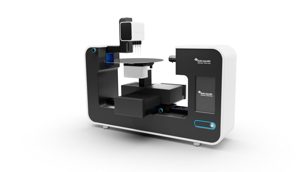
Biolin Theta Wafer Optical Tensiometer

Theta Wafer

Premium optical tensiometer for fully automated contact angle measurements on...

Smart SE
BCS-975R Premium — Battery Cyclers | NewRoad

Smart SE

The HORIBA Smart SE is a compact, portable spectroscopic ellipsometer...

Auto SE
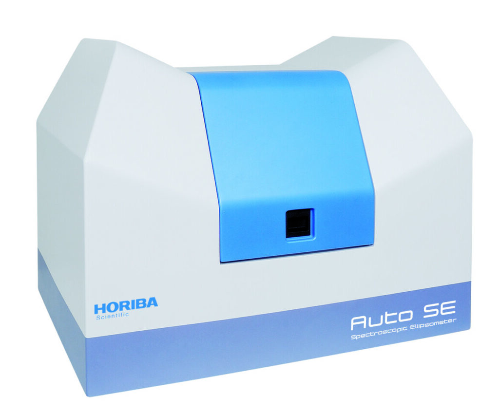
HORIBA Auto SE Ellipsometer

Auto SE

The HORIBA Auto SE is an automated spectroscopic ellipsometer optimized...

UVISEL Plus
BCS-975R Premium — Battery Cyclers | NewRoad

UVISEL Plus

The HORIBA UVISEL Plus is a spectroscopic ellipsometer covering the...

PowerArc
BCS-975R Premium — Battery Cyclers | NewRoad

PowerArc

The HORIBA PowerArc is a high-power xenon arc lamp illuminator...

iHR series
BCS-975R Premium — Battery Cyclers | NewRoad

iHR series

The HORIBA iHR series are high-resolution imaging spectrometers and monochromators...

APPLICATIONS

KEY CHALLENGES

Characterizing ultra-thin films with sub-nanometer accuracy, detecting trace contamination on wafer surfaces, evaluating wettability for photolithography processes, monitoring etch and deposition uniformity, and ensuring the quality of dielectric and metal interfaces are among the most demanding measurement requirements in semiconductor manufacturing.

NEWROAD SOLUTIONS

QCM-D and thin-film analysis instruments provide precise mass and viscoelastic characterization of deposited films. Contact angle analyzers evaluate wafer surface cleanliness and treatment effectiveness for lithography and bonding processes. Surface energy measurements support adhesion optimization in advanced packaging workflows.

EXPLORE TECHNOLOGIES

Raman

Raman Spectroscopy is a non-destructive analytical technique used to identify molecular composition, chemical structure, and material properties.

Lights prisms effect close up | NewRoad

AFM

A scanning probe technique that images and measures surface properties at the nanometer scale by detecting tip-surface forces — operating in air, liquid or vacuum without special sample preparation.

Close up violet foam blob | NewRoad

Elemental Analyzer

X-ray fluorescence and glow discharge spectroscopy provide fast, accurate multi-element composition analysis of solid materials and thin films, from bulk characterization to nanometer-scale depth profiling.

Spectroscopy

Measurement of light absorption, transmission and reflectance across the ultraviolet, visible and near-infrared spectrum — for chemical identification, concentration measurement and process monitoring.

Colorful light prisms reflection | NewRoad

Vibration Isolation Systems

Passive and active vibration isolation platforms protect precision instruments from environmental disturbances, ensuring sub-nanometer measurement stability in AFM, interferometry, and other high-resolution techniques.

This site is registered on wpml.org as a development site. Switch to a production site key to remove this banner.