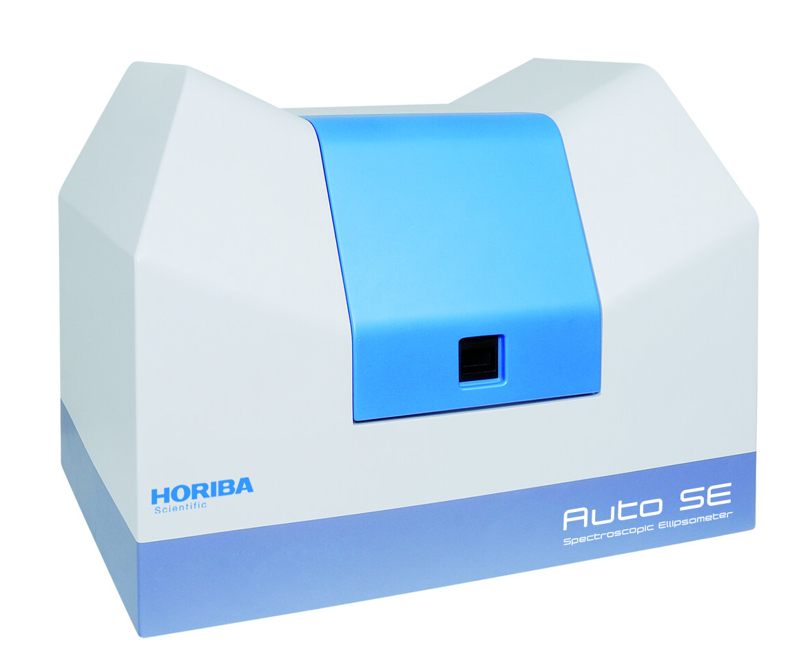
The HORIBA Auto SE is an automated spectroscopic ellipsometer optimized for production environments and high-throughput thin film characterization, combining fast measurement speed with high accuracy for wafer-scale quality control and process monitoring.
The HORIBA Auto SE is a spectroscopic ellipsometer designed for automated, high-throughput thin film measurement in production environments, R&D lines, and quality control laboratories where measurement speed, repeatability, and automation capability are critical. Building on HORIBA’s ellipsometry expertise, the Auto SE combines a fast rotating-analyzer ellipsometer with a spectrographic detector to acquire full spectral ellipsometry data simultaneously across the visible range without mechanical scanning, allowing measurement times well under one second per point. This speed enables high-throughput wafer mapping (measuring tens to hundreds of points per wafer for uniformity and thickness maps), inline process monitoring, and rapid feedback for process control. The Auto SE is designed for simple, repeatable sample loading and positioning, with software that enables recipe-driven automated measurements, batch processing, and integration with factory automation systems. The optical design provides accurate, reproducible measurement of SiO2, Si3N4, polysilicon, metal films, photoresists, and other process-relevant thin films commonly encountered in semiconductor and MEMS fabrication. Results — thickness, refractive index, and optical constants — are extracted automatically using pre-loaded material libraries and measurement recipes. The instrument connects to DeltaPsi2 or WINSEMIAN software for data management and statistical process control (SPC) analysis. NewRoad provides the HORIBA Auto SE in Israel for semiconductor fabs, MEMS manufacturers, photovoltaics production, and R&D thin film laboratories requiring fast, automated thin film characterization at production scale.
WHY CHOOSE THIS PRODUCT
High-throughput automated ellipsometry for production and quality control environments
Fast simultaneous spectral detection — sub-second measurement per point for wafer mapping
Recipe-driven automation for batch processing and factory integration
Accurate measurement of process films: SiO2, Si3N4, metals, photoresist, polysilicon
DeltaPsi2 / WINSEMIAN software for SPC integration and data management
A comprehensive suite of surface, electrochemical, and structural characterization instruments enables materials scientists to understand, optimize, and validate the properties of advanced materials.
Nanotechnology
Semiconductors
High-sensitivity surface and thin-film characterization instruments are essential for semiconductor wafer processing, yield optimization, and failure analysis at the nanoscale.
RELATED PRODUCTS
Explore Similar Solutions
Browse related instruments and complementary solutions selected for your research and application.